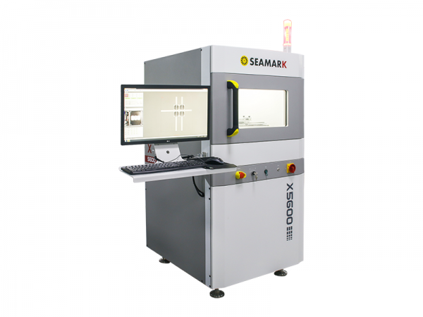
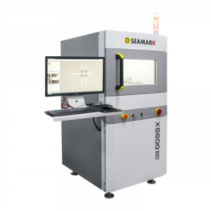
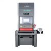
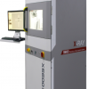
PCB X-RAY INSPECTION SYSTEM X5600
Call us
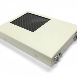
Miniaturized equipment, easy to install and operate
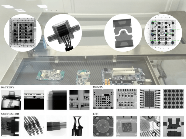
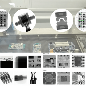
Applicable to Chip, LED, BGA/CSR Wafer, SOP/QFN, SMT and PTU packaging, Sensors, Connectors, and Precision Castings inspection.
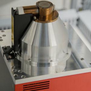
High resolution design to get the best image in a very short time.
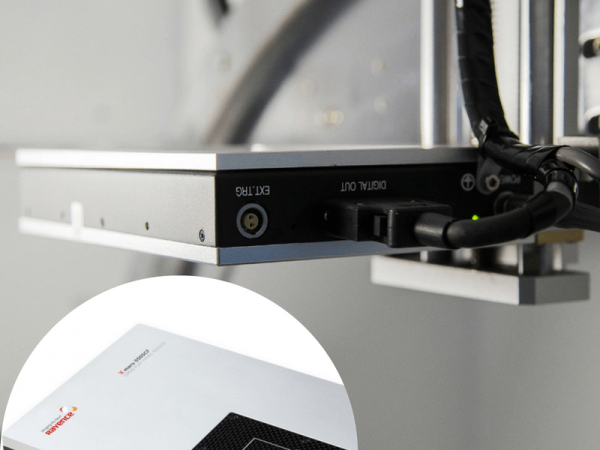
Infrared automatic navigation and positioning function can select the shooting location quickly.
CNC inspection mode which can quickly and automatically inspect multi-point array.
Inclined multi-angle inspection makes it easier to inspect sample defects.
Simple softwareoperation, low operating costs
Long lifespan
Delivery time 3 weeks
Hotline: +84 988 919 818
+84 769 116 968
Email: cuong@smt-vn.com
sales@smt-vn.com
Application
1) Defect inspection in IC encapsulation, e.g.: layer separation, cracking, void, and line integrity.
2) Measuring chip size, measuring line curvature, measuring the proportion of solder area of components.
3) Possible defects in PCB manufacturing processes, e.g.: misalignment, solder bridge and open.
4) SMT solder short, cold solder, component shifted, solder insufficient, solder void inspection and measurement.
5) Defect inspection of open, short or abnormal connections that may occur in automotive wiring harnesses and connectors.
6) Inner rupture or hollow inspection in plastic or metal.
7) Battery stacking uniformity, electrode welding inspection.
8) Seed, biological material inspection etc.
Please note: Specification are subject to change without notice!
Enhanced BGA Inspection Function
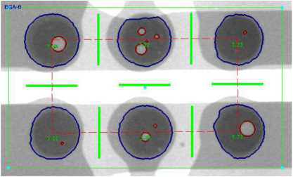
Automatic Void Ratio Calculation
X5600 can quickly select and mark a single solder ball, or select the solder balls to be inspected by matrix box;it can manually or automatically identify BGA solder balls and complete the inspection. Follow the system guidelines to easily complete the inspection process and ensure accurate and reliable inspection results.
Advanced Measuring and Defect Detection Tool
■Automatically detect defects
X5600 can automatically detect size, area, broken wire, bridging etc.
■Customize image algorithm
Customize software algorithms based on product features and request to achieve fully automatic defect inspection algorithms, including Y/N, crack, broken wire, offset, size, and quantity etc.
■ Measuring tools
Distance, distance ratio, lines distance, angle, arrow mark, circle radius, points distance, circle centers distance, circumference, hand-drawn polygon, hand-drawn freeform etc., can add text description.

CNC Inspection
■CNC automatic operation inspection
X5600 support CNC multi-point automatic
inspection mode, based on product feature set multi-point coordinates for automatic inspection.
■Automatic CNC operation detection
Automatically save images, generate reports, also
support batch inspection.

Tilt/Rotate Function
■Tilt angle inspection function
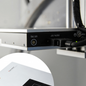
The X5600 detector support a tilt angle of ±30°. For cases where the photo taken on the front of a special device cannot identify the defect feature, the tilt function can be used to observe the device features at multiple angles, making it easier to analyze and identify the defect.
■360°Rotating photo inspection function
Equipped with a rotating manipulator that can rotate 360 degrees to take images, no dead angle for defects observation.


Reviews
There are no reviews yet.